What a panel is made of
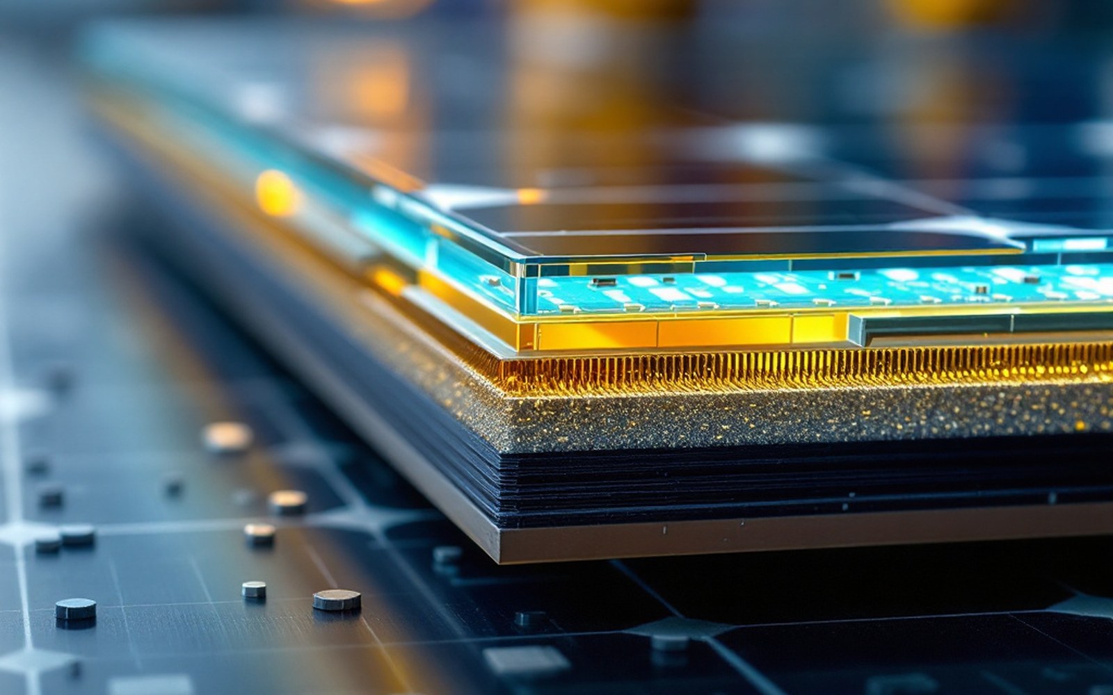
The five materials that do the work
A photovoltaic module looks simple from the outside: a sheet of glass, a frame and some wires. Take it apart and you find five materials doing specific jobs, each with its own supply chain and each adding to the cost. Get one wrong — too thick, too impure, wrong alloy — and the panel underperforms or fails early. The industry's decades of cost reduction, tracked by researchers at the Fraunhofer Institute for Solar Energy Systems and the National Renewable Energy Laboratory, have been an exercise in optimising all five simultaneously.
Glass is the front sheet, and it is the heaviest single component in a standard panel — roughly 65 to 70 percent of total mass. It has to transmit light efficiently, resist hail, shed water, and last thirty years in full sun without significant yellowing or delamination. Solar glass is low-iron, because ordinary float glass contains enough ferrous oxide to absorb a measurable fraction of the spectrum. The iron content is brought below 0.02 percent, and the surface is usually textured — etched or cast with a fine pyramid pattern — to reduce reflection. A 60-cell panel uses roughly 3.2 mm of glass, a spec that has barely changed in two decades because the physics and the economics of thinner glass argue in opposite directions: thinner saves weight and material, but makes the module more vulnerable to mechanical load.
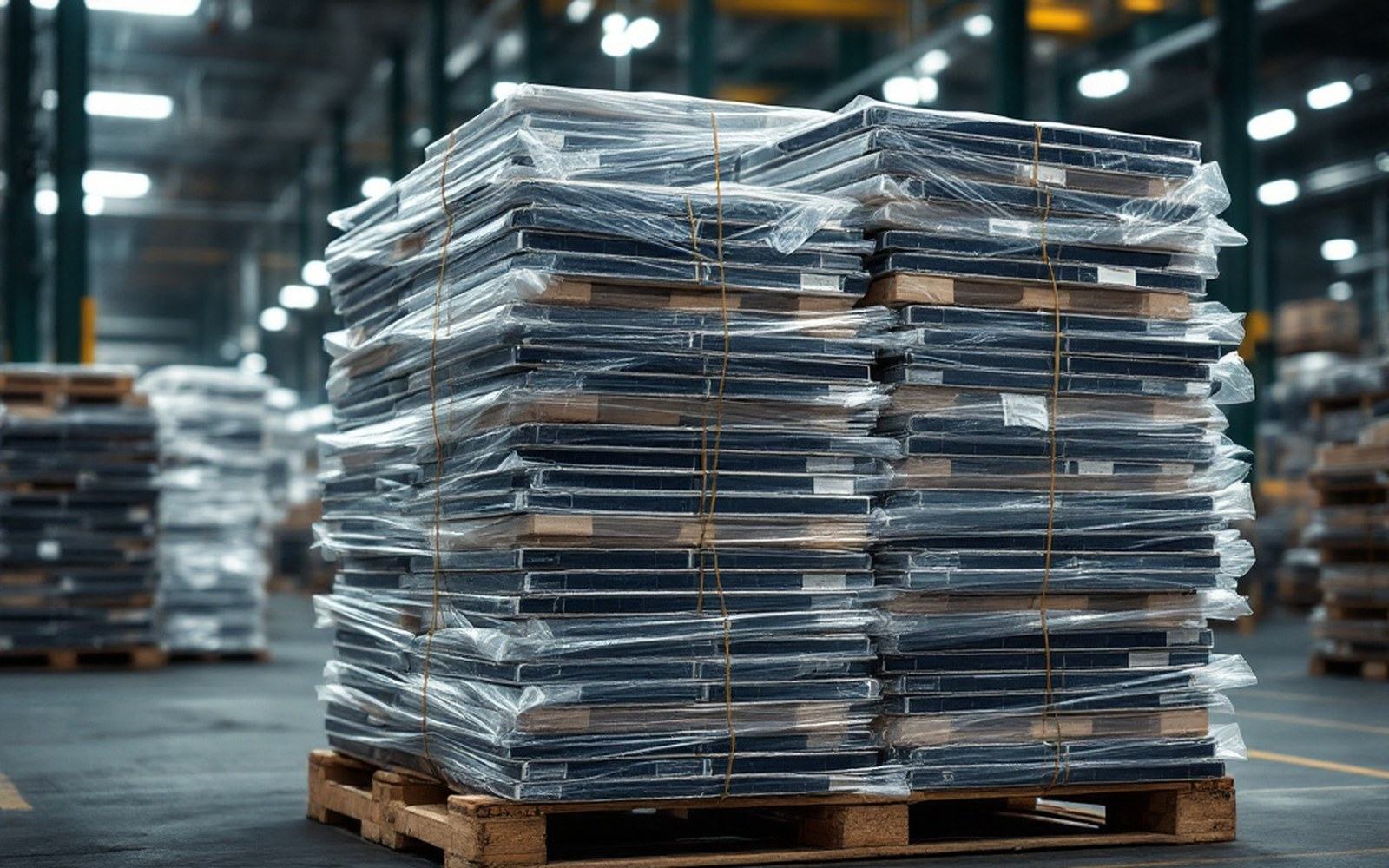
Aluminium forms the frame. It is structural, not electrical — it holds the laminate rigid, allows mounting, and is the part of the panel most likely to be recycled at end of life. The alloy matters: it must resist salt spray and thermal cycling without cracking the bond to the glass edge. Aluminium also appears inside the module as the back-sheet conductor in some designs, though most standard panels use a separate polymer back sheet and print aluminium contacts directly onto the silicon.
The encapsulant is the layer that nobody talks about but that determines how long everything else survives. It sits between the glass and the silicon, and between the silicon and the back sheet, holding the cell in optical contact with both surfaces and sealing out moisture. Ethylene-vinyl acetate — EVA — is the dominant material, a polymer that is cast as a sheet, laid over the cells and laminated under heat and vacuum until it flows around the cell geometry and bonds chemically to both glass and back sheet. The failure mode that matters is acetic acid: as EVA ages under UV and heat, it releases trace quantities of acid that can corrode the silver contacts on the cell below. Managing this degradation — keeping it below 0.5 percent annual power loss — is why module warranties exist and why the research into alternative encapsulants such as polyolefin films is active at institutions including Lawrence Berkeley National Laboratory.
Silicon: the dominant material and the one that changed most
The photovoltaic cell is a slice of silicon, and for most of the industry's history it was sliced from a grown crystal — a boule pulled from a melt in a Czochralski furnace, then sawn into wafers roughly 180 micrometres thick. The sawing itself destroyed material: the kerf loss from a wire saw could consume as much silicon as the finished wafer. Reducing wafer thickness and improving wire-saw technology were two of the cost levers that drove the learning curve down through the 1990s and 2000s.
Polycrystalline silicon — cast rather than pulled — was for years the industry standard because it was cheaper to produce, accepting lower crystal quality in exchange for a simpler process. Since roughly 2018, monocrystalline wafers, produced by a Czochralski process operating at very high purity, have reclaimed market dominance. The reason is efficiency: a monocrystalline PERC cell (passivated emitter and rear contact) converts more of the incoming spectrum because minority carriers — the electrons and holes generated by photons — travel further before recombining. Higher efficiency means fewer panels per megawatt, which reduces the cost of glass, aluminium, encapsulant, racking and labour proportionally. The silicon itself became the cheaper choice once the balance-of-system savings were counted.
A standard 60-cell module in 2010 used around 400 milligrams of silver per cell, putting a panel's total silver content above 20 grams.
The raw material — metallurgical-grade silicon — is produced by reducing quartz in an electric arc furnace, then refined to semiconductor-grade purity by the Siemens process, driving the silicon content above 99.9999 percent. That refining step is energy-intensive and geographically concentrated. Producing the purified polysilicon feedstock consumed by a single gigawatt of cells requires roughly 5,000 to 6,000 tonnes of material and substantial electricity, which is why the industry has historically clustered polysilicon production where power is cheap.
Silver: the constraint
Of the five materials, silver is the binding constraint — not because it is scarcest in the ground but because demand for solar manufacturing has grown faster than the industry can reduce the amount of it per panel. Silver is the electrical contact material: fine lines are screen-printed onto the front face of each cell to collect current from the illuminated surface. The lines must be fine enough not to shade significant area but conductive enough not to waste power to resistance.
A standard 60-cell module in 2010 used around 400 milligrams of silver per cell, putting a panel's total silver content above 20 grams. By 2023, incremental improvements — finer screen meshes, higher-solids pastes, multi-busbar and shingled cell designs — had brought that figure down to around 10 to 13 milligrams per cell, or roughly 600 to 800 milligrams for the whole module. The trajectory continues, with IRENA and the International Energy Agency both tracking silver intensity as a materials constraint because solar manufacturing now consumes roughly 10 percent of annual global silver supply, a share that rises as deployment accelerates.
The industry response has two tracks. The first is further paste optimisation: silver-coated copper particles can partly substitute for pure silver in some contact formulations, reducing cost without significant efficiency penalty. The second is architectural: heterojunction cells and back-contact designs move some or all of the silver away from the front surface, reducing shading and sometimes allowing lower-grade silver to be used, though the manufacturing process is more demanding. Richard Swanson, whose work on point-contact solar cells in the 1980s at Stanford University laid groundwork for back-contact architectures, described the core tension between contact conductivity and optical shading in terms that remain directly applicable to today's engineering choices.
Back-contact and heterojunction modules carry higher silver intensity per unit area than mainstream PERC cells, which means the silver constraint is not resolved by moving to higher-efficiency designs — it shifts. What the industry is working toward is a cell architecture that retains monocrystalline silicon's efficiency advantage while reducing silver content below 5 milligrams per cell, a figure that researchers at Fraunhofer ISE regard as achievable within this decade on current development trajectories.
The module, then, is a precision laminate of five materials, each with its own supply chain risk and its own decades-long optimisation history. Glass and aluminium are commodity problems: abundant, globally traded and unlikely to constrain deployment. EVA supply is tight in high-demand periods but responds to capacity investment. Silicon refining is energy-intensive and geographically concentrated. Silver is the number that the whole industry watches most carefully, because it is the one where the physics of contact resistance and the economics of a finite metal are pulling hardest against each other.